Product Center

Gaming peripherals
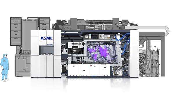
Why is the chip made for everyone popular in the past so expensive? Not only is it related to its cumbersome production process, but also has a lithography process in the production process of the complete chip, and this program requires hundreds of millions of lithography machines. A machine needs hundreds of millions of dollars. Why do you need to be so expensive? Let's take a look at what a lithography machine is and how it works.
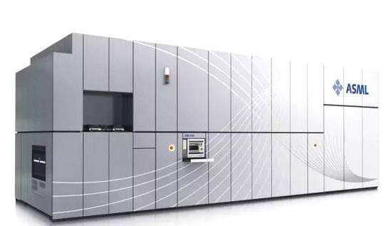
What is a lithography machine?
The lithography machine is one of the core devices for chip manufacturing, and is divided into: a lithography machine for producing chips; a lithography machine for packaging; and a projection lithography machine for LED manufacturing. The lithography machine used to produce chips is the biggest shortcoming in the manufacture of semiconductor equipment in China. It can only rely on imported high-end technology. In the first quarter of 2018, Xiamen enterprises imported lithography machines from the Netherlands for chip production equipment.
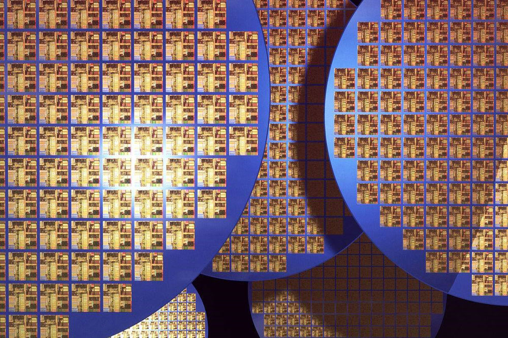
How the lithography machine works
Below we use the lithography schematic to understand the role of each device.
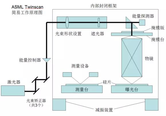
Test stand, exposure stage: workbench carrying silicon wafers.
Laser table: one of the light source and core equipment.
Beam aligner: corrects the incident direction of the light velocity and makes the laser beam as parallel as possible.
Energy Console: Controls the amount of energy that is ultimately applied to the wafer. Underexposure or over-exposure can severely affect image quality.
Beam shape setting: The beam is set to have different shapes such as a circle and a ring, and different beam states have different optical characteristics.
Shader: Prevents the beam from illuminating the wafer when exposure is not required.
Energy detector: Detects whether the final incident energy of the beam meets the exposure requirements and feeds it back to the energy controller for adjustment.
Mask: The device that carries the mask movement, the motion control accuracy is nm level.
Objective lens: compensates for optical errors and reduces the circuit diagram ratio.
Wafer: A wafer made of wafers.
Internal closed frame and pressure reducer: isolate the workbench from the external environment, maintain the level and reduce external interference.
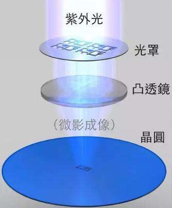
In the process of processing the chip, the optical machine projects the beam through the mask of the circuit diagram through a series of light source energy and shape control means, compensates various optical errors through the objective lens, and scales the circuit diagram to be mapped to silicon. On-chip, and then chemically developed to obtain a circuit diagram engraved on the silicon wafer. Generally, the lithography process is subjected to the steps of cleaning, drying, coating, spin coating, soft baking, development, hard baking, laser etching, etc. of the silicon wafer surface. The chip after one photolithography can continue to be glued and exposed. The more complicated the chip and the number of layers of the circuit diagram, the more precise the exposure control process is.
Status of lithography machine
At present, the Netherlands ASML is the leader in the field of lithography machine, occupying 80% market share, monopolizing the high-end lithography machine market, the most advanced EUV lithography machine also depends on ASML production, and China's current leading lithography machine Manufacturers can only produce 90nm chip lithography machines for processing, the technology is very different, so want to have high-end lithography machines can only rely on imports, which is why lithography machines are so expensive. Therefore, in order to reduce costs and strengthen the development of China's semiconductor industry, it is necessary to solve the problem from the source, develop high-end equipment, in order to better manufacture chips, and thus constitute devices, in order to change the status quo.
Long press the identification QR code to follow us~
Come at a speed, because of beauty
About Ramsta
Ruishi International Headquarters is located in Hong Kong and Taiwan. It has set up a research and development center in Shenzhen. It has set up a sales company in Shenzhen. It has a storage product R&D and manufacturing base in Taiwan and Shenzhen. It is committed to the research and development and manufacturing of high-end, cutting-edge storage products. Rui Shi established the Greater China Marketing Center in Shenzhen. As a professional storage product R&D, manufacturing and sales integration service provider, Ruishi currently has a place in the SSD solid state drive, DARM module memory, TF flash card and other series of storage products.
